Prototipos de PCB de forma sencilla
Servicio completo para prototipos de PCB personalizados.
9:00 - 18:00, Mon.- Fri. (GMT+8)
9:00 - 12:00, Sat. (GMT+8)
(Excepto los días festivos chinos públicos)
Prototipos de PCB de forma sencilla
Servicio completo para prototipos de PCB personalizados.
9:00 - 18:00, Mon.- Fri. (GMT+8)
9:00 - 12:00, Sat. (GMT+8)
(Excepto los días festivos chinos públicos)
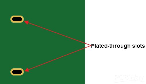
Plated-through slots (PTS) are holes in PCBs that have been electroplated with conductive material. PTS are used to provide electrical connections between different layers of the PCB. This article will introduce PTS from four aspects: definition, advantages, design considerations, and manufacturing process.
Plated-through slots refer to copper-plated slots that can be used for electrical connections and are a way to achieve through-hole plating on a printed circuit board (PCB). Plated through slots are the electroplating within the PCB, while the electroplating on the outer edge of the PCB is called edge plating.
The slots can be defined as plated through holes (PTH) or non-plated through holes (NPTH). Each top and bottom connection between milling and copper will produce a plated through hole (PTH). Plated-through slots are used for through-hole device pins, and both plated-through slots and non-plated-through slots can be used on a PCB.

Plated-through slots can be used to better accommodate rectangular-pinned components, as opposed to using standard round holes which may result in wasted space. Plated-through slots offer several advantages, including:
• Reducing unnecessary gaps between component pins and the PCB, allowing for a more compact and space-saving design.
• Minimizing the chance of soldering gaps. When slots are used for large rectangular leads, there will be no unnecessary gaps left after component placement.
• Precise lead slots can also free up more space on the surface of the PCB.
During the design phase, it is necessary to specify the exact length and width of each plated-through slot and annotate them in the manufacturing drawing to help the manufacturer understand the specific requirements for production.
In EDA tools, an elliptical hole can be added to define a plated-through slot. Plated-through slots can also be defined in the Gerber mechanical layer. If the design file does not include a mechanical layer, a mechanical layer should be added and the hole defined within it. Additionally, it is recommended to use a README file to clearly document the requirements for plated-through slots.
PCBWay offers a minimum width of 0.5mm for plated-through slots and 0.8mm for non-plated-through slots. The first step in creating such slots is to use milling processes to cut out slots of the required size from the PCB material. This process removes any unwanted copper from the surface of the board, forming the required solder pads, traces, and other structures. Next, the slots are drilled out using an appropriate drilling method according to the design requirements, and the slots are cleaned to remove any residue. Then, these slots are plated with copper using a chemical plating method, similar to through-hole plating. Finally, the slots are surface treated.
When dealing with through-hole devices that have rectangular or unconventional pins, selecting through-holes will create additional unnecessary space within the holes. To avoid this situation, the ideal approach is to create a slot with a shape that is exactly the same as the pins, which provides a better fit.