Prototipos de PCB de forma sencilla
Servicio completo para prototipos de PCB personalizados.
9:00 - 18:00, Mon.- Fri. (GMT+8)
9:00 - 12:00, Sat. (GMT+8)
(Excepto los días festivos chinos públicos)
Prototipos de PCB de forma sencilla
Servicio completo para prototipos de PCB personalizados.
9:00 - 18:00, Mon.- Fri. (GMT+8)
9:00 - 12:00, Sat. (GMT+8)
(Excepto los días festivos chinos públicos)
In the PCB industry, side plating, sometimes called Castellation or Edge plating, refers to the metallization of the edges of a circuit board. In other words, side plating refers to the copper plating that runs from the top to the bottom surface of the board and along one or more peripheral edges. The surface treatment for side plating can be ENIG, ENEPIG, HASL, or any other surface treatment that provides electrical connectivity. With side plating of printed circuit boards, the PCB edge is used for technical features of the later assembly. Portions of the PCB's outline and interior areas can be metalized.

Need to improve the conductivity of the PCB
Need to make connections on the edge of the PCB
Need to prevent lateral impact
Secondary PCB is connected to the main board through the edge
Need to solder the edge to improve assembly

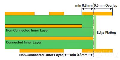
To ensure the manufacturability of side plating, overlapping copper (i.e. copper surfaces, pads or traces) should be used to define the metalized areas in CAD layout file. The following rules should be followed:
The minimum overlap value should be 0.5mm.
For the connection layers, a minimum of 0.3mm of a connecting copper line must be defined.
On non-connection layers, the copper should be kept at least 0.8mm apart from the edge of outer contour.

In high-frequency circuit boards, the quality of signals is critical to the performance of the circuit. Therefore, Side Plating is very useful in this case.
Side plating enhances the electromagnetic compatibility (EMC) of multilayer PCBs.
Side plating plays a role in shielding the inner layers of the PCB, reducing external signals' interference with the circuit board. Therefore, Side plating can minimize external sources' interference with the circuit board.
Boards with Side plating can prevent electrostatic damage during transportation.
Because the manufacturer needs to fix the PCB in the production panel during the process, they will not be able to plate the entire length of the edge. Therefore, some gaps are required when placing the rout label. Manufacturing circuit boards using edge plating requires the layout of the circuit board where edge plating is required before starting the through-hole plating process. This precludes V-cutting scores on plates that require edge plating.
Usually, we recommend customers to make immersion gold or immersion silver for edge plating. When designing the solder mask layer, it should be solder mask opening in the file. Also, you can show us some texts to show the detailed requirements.
As a PCB service provider with over a decade of experience in PCB manufacturing, fabrication and assembly, PCBWay has a rich background.If there is a demand for side plating boards,please feel free to contact us!
More information please check here: