Prototipos de PCB de forma sencilla
Servicio completo para prototipos de PCB personalizados.
9:00 - 18:00, Mon.- Fri. (GMT+8)
9:00 - 12:00, Sat. (GMT+8)
(Excepto los días festivos chinos públicos)
Prototipos de PCB de forma sencilla
Servicio completo para prototipos de PCB personalizados.
9:00 - 18:00, Mon.- Fri. (GMT+8)
9:00 - 12:00, Sat. (GMT+8)
(Excepto los días festivos chinos públicos)
When stacking a PCB, layer orientation can be used to help PCB manufacturers differentiate between different layers. This is because many layout programs allow mirrored data output, which can cause production problems if there are no clear layer labels or if the layer labels are incorrect. To ensure the correct production of the PCB, unique and correct labels should be used to indicate the TOP and BOT on the PCB.
Now, let's have a look at the vital guidelines that should be followed to obtain the correct layer orientation.
A PCB consists of multiple layers that are stacked together, including substrate layers, copper layers and prepreg layers. These layers are combined to form a stack-up, and the number of layers required depends on the design needs of the PCB. Different PCBs may require different numbers of layers to meet their functional requirements.
To help manufacturers understand the sequence and direction of each layer, a physical label must be etched on each layer, which helps to locate all the layers when stacking the PCBs. This is known as layer orientation in PCB.
If the design software has already correctly positioned and ordered all the layers, why is there a need for physical labels? In fact, this is for the convenience of placing the layers and supporting visual inspection. When the layers are properly labeled, a simple visual inspection can identify errors in orientation and direction, which ultimately helps to place components correctly.
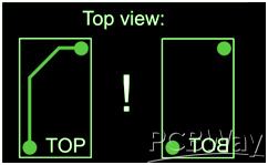
A set of universal standards should be followed when labeling to avoid misunderstandings. The top layer is typically labeled as "TOP" while the bottom layer is labeled as "BOT" (in mirror image form).
When viewed from the top of the design file, we need all the top and inner layers to appear as a true board in normal visual form, but for all the bottom layers, a mirrored visual is required.
The following diagram is an example:

The caption "Layer 1" to "Layer 4" are used for clarity purposes only.

Layer orientation is crucial for PCB manufacturers during the stacking process. Don't forget to label each layer with the corresponding orientation. If you still have questions about layer orientation, please feel free to contact us.
More information please check here: