Prototipos de PCB de forma sencilla
Servicio completo para prototipos de PCB personalizados.
9:00 - 18:00, Mon.- Fri. (GMT+8)
9:00 - 12:00, Sat. (GMT+8)
(Excepto los días festivos chinos públicos)
Prototipos de PCB de forma sencilla
Servicio completo para prototipos de PCB personalizados.
9:00 - 18:00, Mon.- Fri. (GMT+8)
9:00 - 12:00, Sat. (GMT+8)
(Excepto los días festivos chinos públicos)
PCB panel is a consideration for both PCB manufacturing and PCB assembly cause some boards are irregular. The panel can reduce the time and labor for production and testing.
PCBWay, as the most professional manufacturer in this field for more than a decade. We can make the boards according to your panel design. Also, we can provide the service to help you panel the single board for free.
That means we help you connect the single boards(same or different are both OK) on one big panel by different route process, then it will be easy for you to break them into single PCB. For the routing process, it has three types: V-scoring, Tab route, and stamp holes.
Panel with V-Cut/V-Scoring/V-Groove
For V-scoring panelization, space between boards can be 0mm or 2mm. Please take following images as reference.


V-scring has to be continuous and can not be stopped in panel, if you have many different boards like following image to be panelized, we suggest add tab routes between boards instead of V-scoring.
V-scoring is the most popular way in the PCB panel. V-scoring is the v-shape line to connect boards for convenience separation. We also require the v-scoring boards, please observe the following rules:
The gap between the individual circuit boards in the layout is 0mm based on the minimum spacing between copper pattern (trace/pad/copper ground) and V-cut line is 0.4mm.
Scoring lines must be straight; horizontal and vertical lines are possible, so the board's frame must be regular, and the size of boards must be over 45mm*60mm.
For stability, We recommend using V-scoring only for board thicknesses greater than 0.6mm.

More information about V-scoring,please check PCB V-Scoring.
For tab route and stamp holes, it can be used in the irregular boards. However, For the tab route, the space between boards should be 1.6mm.

Panel with Tab Route
For panel with tab routes, 1.6mm space is needed between boards. There are 2 kinds of tab routes be used for panel. One is tab route with breaking holes(stamp holes) and the other one is tab route with tab(no holes).
Tab route with breaking holes(stamp holes)
For tab route with breaking holes diameter should be ≥0.45mm, regular diameter is 0.55mm-0.6mm. Holes space has to be ≥0.35mm, usually we will add 5-6 holes to each tab, please take following image as reference.

Tab route with breaking holes
Tab route with tab
Tab route with tab,tab width has to be at least 2mm, please find following image.

Tab route with tab
Breakaway rail, also called edge rail, is a rail at the edge of panel boards to fix the panel boards on a machine more easily. So it is usually used in assembly PCB boards. For breakaway rails, you can also use a v-scoring or tab route to connect then you can cut the rails easily after assembly. In our factory, our mini edge rail is 5mm. Please see the following picture.

Mass production: If you need to build a large number of PCBs, panelization will save you time and money.
Product Safety: Panelization protects the PCB from shock and vibration during assembly.
Speed and efficiency: From paste printing to component assembly, soldering, and even testing, as part of a large array, processing multiple boards at once is faster and more efficient.
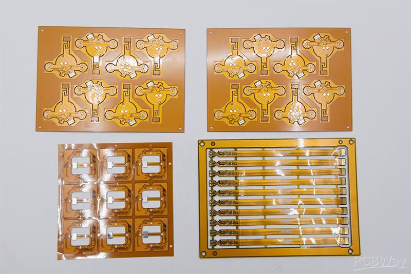
In the production process of FPC flexible circuit board, in order to save cost, improve production efficiency, shorten the production cycle, often use the method of panel production, rather than single chip production. Generally, FPC flexible circuit boards have three panel methods, namely, conventional panel, oblique panel and backward panel. All panel methods must follow the principle of material saving under the premise of production.

In FPC flexible PCB panel, you need to know those following principles:
On the premise of each process can be produced, as far as possible ' squeeze '. The so-called ' extrusion ' is to reduce the distance between board and board, so as to reduce the size of the whole panel, save production materials and reduce production costs
The distance between the single plate is at least greater than 2mm, which is to meet the needs of placing positioning holes. In the process of mass production, the molding generally adopts the way of die-punching. In order to enhance the accuracy of die-punching, the positioning holes need to be placed between each piece in the panel to avoid the deviation of die -punching and lead to FPC scrap. In the process of sample production, laser cutting molding is generally used. In order to avoid slight deviation and prevent the occurrence of one deviation and the whole deviation, the chips cannot be directly connected, so that they do not affect each other.
A panel need to add etching characters, the size of the plate, the number of simple instructions, so as to facilitate subsequent production check and calibration.
The positioning hole is added in the four corners of the whole panel, and a corner is selected to mark different positioning holes, which is convenient for the subsequent production process to keep the direction consistent, so as not to cause the sealing film back, character printing and so on.
The width of the panel is fixed to 250 mm, and the length is within 250 mm as far as possible. The larger the size of the panel, the greater the offset, the worse the production accuracy, and the higher the product failure rate.
Next, let's learn more about panelization through the following video:
More information please check here: